


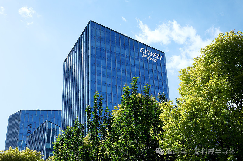
Aikwei Semiconductor: Empowering the Entire Semiconductor Industry Chain Innovation with Domestic Equipment
Aug 26,2025
17 Years of Accumulation: Domestic Equipment Hard Power
Exwell's technical foundation can be traced back to the semiconductor equipment R&D team launched in 2007. After eight years of technological accumulation and industry cultivation, the Hunan company was officially registered in 2015 and has now grown into a national high-tech enterprise. It has formed a core technical team led by senior experts, gathering technical forces from top domestic research institutions, creating R&D and production capabilities covering integrated circuits, discrete devices, 5G communications, optoelectronic devices, sensors, and other fields.
The company has built a 1,500-square-meter Class 10,000 cleanroom and a 1,000-square-meter Class 1,000 clean laboratory, establishing a full-process solution system from device R&D to mass production. By 2025, it has obtained over 60 patents and software copyrights (including 10 authorized invention patents), breaking through multiple foreign technology blockades; it has passed ISO9001 quality management system certification and SEMIS2 safety certification, with equipment performance and stability reaching international first-class standards. It currently serves over 300 enterprises including Huawei, CRRC, CETC, and its research clients cover more than 90% of the semiconductor field's "Double First-Class" universities.
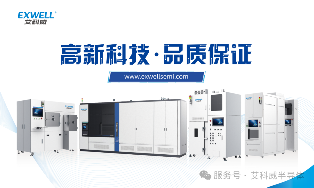
02 Equipment Matrix: Unlocking Core Processes
Vertical Oxidation Diffusion Annealing Furnace
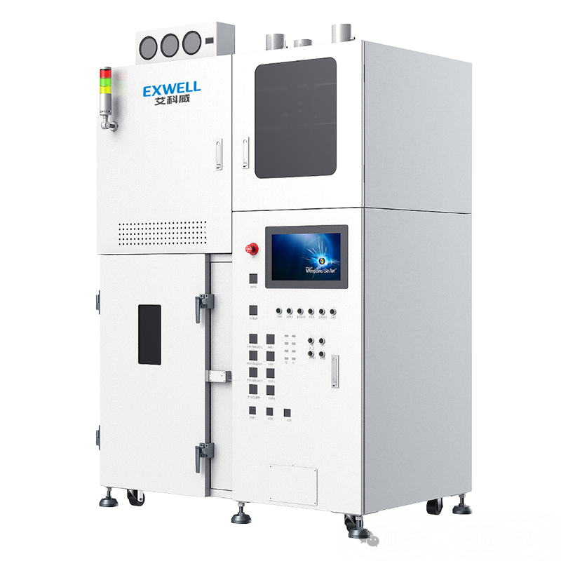
Equipment Features:
High-precision humidity (oxidation) temperature control Uses a professional temperature control system to precisely regulate the mid-zone temperature, with options for fully automated or manual machines, meeting both efficient production and small-batch innovative R&D needs.
Advanced particle contamination control: Class 1,000 assembly workshop, EP-grade pipelines, combined with efficient purification technology to reduce particle interference during the process, ensuring wafer interface quality.
High reliability system design: Stable equipment operation meets the precise process requirements for optoelectronic device fabrication.
Application scenarios:
Applicable materials: semiconductor substrates such as silicon, lithium niobate, compounds, etc.
Applicable processes: mainly used for oxidation, diffusion, annealing (including alloy annealing), and chemical vapor deposition (LPCVD) processes.
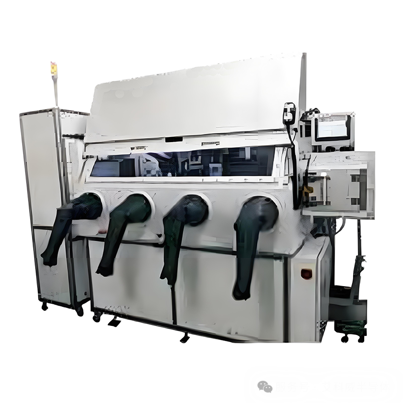
Horizontal Oxidation Diffusion Annealing Furnace
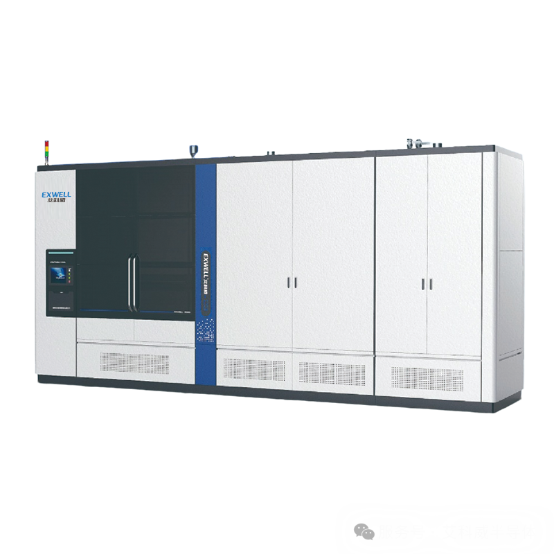
Equipment Features:
Flexible multi-process combination configuration: Supports switching among oxidation, diffusion, annealing, and other processes to meet diverse needs.
Mature and stable equipment architecture: Market-validated design ensures long-term reliable operation.
High reliability process output: Meets the requirements for electrical characteristic control of semiconductor materials and device structure fabrication.
Application scenarios:
Applicable materials: silicon, silicon carbide, and other semiconductor materials. Applicable processes: mainly used for oxidation, diffusion, annealing (including alloy annealing), and chemical vapor deposition (LPCVD) processes.
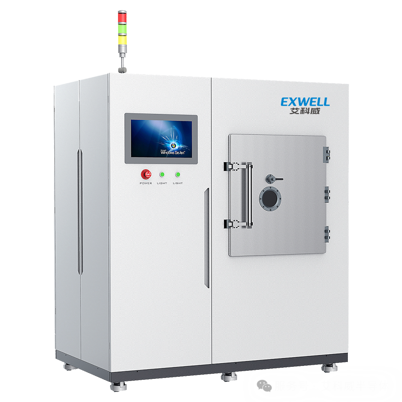
PVD Magnetron Sputtering Coater
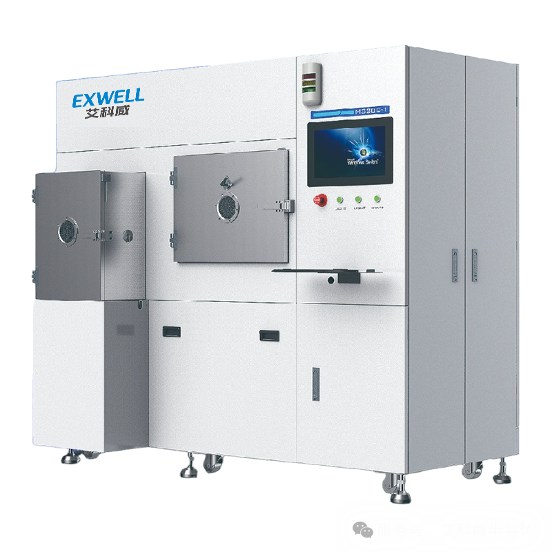
Equipment Features:
High-precision temperature control capability: Substrate table temperature control adapts to the temperature requirements of different material film depositions.
Advanced particle contamination control: Chamber design reduces particle interference during coating, improving film purity.
High capacity and automation integration: Suitable for mass production, supporting the preparation of films from metals, dielectrics, and other materials.
Application scenarios:
Applicable materials: substrates such as silicon, compound semiconductors, ceramics, quartz, etc.
Applicable processes: magnetron sputtering coating used for preparing metal (e.g., Al, Au) and dielectric (e.g., SiO₂, ITO) films. Applicable fields: integrated circuit electrode fabrication, optoelectronic device film deposition.
Reactive Ion Etcher (RIE)
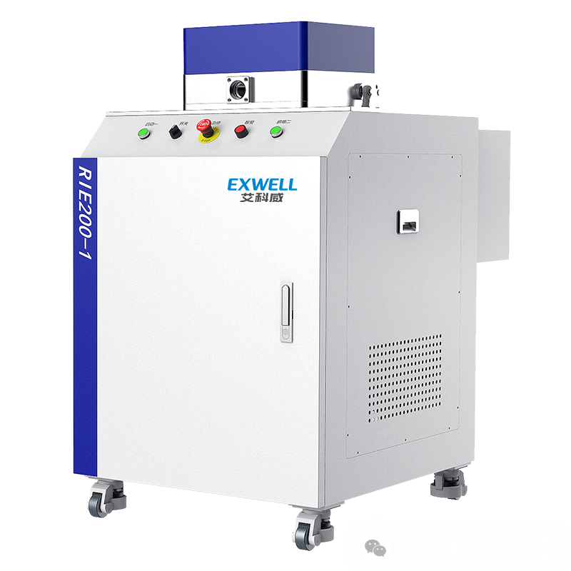
Equipment Features:
Digital intelligent control: Fully digital automatic control of the process, easy to operate and learn.
Constant pressure automatic control: Automatic adjustment of reaction pressure to ensure process repeatability and stability.
Configurable loadlock loading chamber: Reduces atmospheric contamination, improves loading efficiency and chamber vacuum maintenance.
Application scenarios:
Applicable materials: silicon, silicon dioxide, silicon nitride, etc.;
Core processes: transistor gate etching, MEMS structure processing, contact hole etching;
Application fields: integrated circuit manufacturing, microelectromechanical systems, optoelectronic devices.
Ion Beam Etcher (IBE)
Equipment Features:
Dual-mode workpiece table: Single-piece (angle adjustable from -90 to 90°) and multi-piece (rotational) types, suitable for research and mass production needs.
Water-cooled low-temperature etching: Water-cooled worktable design, stable temperature control achieves low-temperature wafer etching, effectively reducing thermal damage risk.
Application scenarios:
Applicable materials: Metals, ceramics, compound semiconductors, quartz, etc.;
Core processes: Brittle material etching, nanostructure processing, ion milling;
Application fields: Optoelectronic devices, quantum chips, micro-nano optical components.
Laser Sealing and Welding Machine
Equipment Features:
High-reliability laser source: Imported lamp-pumped YAG solid-state laser with stable performance.
Precision CNC Workbench: Precision guide rail + AC servo motor, precise control.
Flexible Trajectory Programming: Welding trajectory programming can be performed according to the shape of the workpiece.
Multi-Workpiece Array System: Welding trajectory simulation demonstration before welding to achieve full-process automatic welding control.
Multi-Workpiece Array System: Supports batch welding to improve production efficiency.
Application scenarios:
Applicable materials: Applicable to metal housings such as cobalt alloy, stainless steel, etc.;
Core processes: Inert gas protected laser welding, hermetic packaging;
Application fields: Packaging of TR components, sensors, optical communication modules.
03 Micro-Nano Platform: Collaborative Implementation of Process Equipment
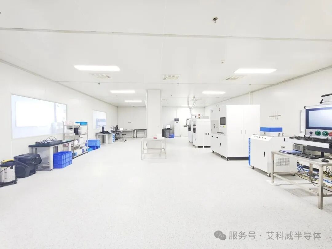
Aikewi has built a 1000㎡ Class 1000 clean micro-nano processing laboratory, integrating core equipment such as oxidation annealing furnace, diffusion furnace, magnetron sputtering coater, and supporting testing instruments including Bruker DEKTAK XT step profiler, Filmetric F20 optical film thickness meter, RTS-9 four-probe sheet resistance meter, and Jingcui optical infrared microscope. It supports verification of oxidation, diffusion, annealing, PVD CVD thin film deposition, etching processes, and collaborates with customers for joint process research and equipment co-development.
The platform serves universities, research institutes, and semiconductor companies by providing process certification services—verifying processes such as wafer diffusion, oxidation, annealing, and metal/dielectric thin film preparation, creating an "industrial-grade trial-and-error field" for parameter optimization and stability testing before equipment mass production.
Adhering to the concept of "process-driven equipment development," the team deeply integrates process requirements into equipment design: achieving precise reproduction of wafer-level processes (such as lattice defect repair, thin film uniformity control), and customizing integrated "equipment + process" solutions for cutting-edge scenarios like quantum chips and MEMS, helping customers shorten R&D cycles, reduce trial-and-error costs, and accelerate technology transfer from laboratory to production line.
04 Equipment Matrix: Unlocking Core Processes
Customer Groups

Research and Education: Covering over 90% of "Double First-Class" universities in the semiconductor field including National University of Defense Technology and Nanjing University, supporting cutting-edge device R&D.
Industrial Customers: Serving more than 300 companies including Huawei, CRRC, CETC, with equipment stably applied in production lines of leading wafer fabs and mainstream semiconductor manufacturers.
Strategic Cooperation
Co-building an "Equipment-Process-Material" collaborative innovation ecosystem with leading companies such as Zhaosheng Microelectronics and Guangxun Technology, jointly tackling "bottleneck" technologies including third-generation semiconductor (silicon carbide, gallium nitride) equipment and 2.5D/3D advanced packaging equipment.
05 Equipment Matrix: Unlocking Core Processes
Aikewi is accelerating the deployment of third-generation semiconductor equipment and key quantum chip process equipment, establishing a Suzhou subsidiary to expand the East China market, and plans to start overseas deployment within three years. Through a doctoral innovation workstation and national-level R&D platform construction, the company will continuously empower the entire semiconductor industry chain with domestic equipment, injecting strong momentum into the autonomy of China's semiconductor industry.
Related News

Service hotline:
+86 0731-88376310
Address: No. 858, Purui West Road, Wangcheng Economic and Technological Development Zone, Changsha City

WeChat official account

Douyin QR code
Online consultation